Computational Quantum Transport in Mesoscopic Systems
Introduction
The ability to reduce the size of electronic circuits to the nanometric scale has lead to increasing interest in the properties of electron transport in the mesoscopic regime, and its dependence on externally tuned parameters. Formation of two-dimensional structures of controllable geometry at semiconductor interfaces, so called electron billiards, sets the experimental grounds for investigating phase coherent electronic transport.
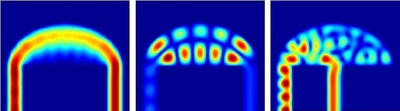
Open quantum billiards
Open semiconductor quantum billiards serve as artificial scatterers of highly tunable characteristics and have pioneered the understanding of the underlying physics, on both experimental and theoretical grounds. They are used to demonstrate and investigate a series of interesting phenomena on the mesoscopic level, such as weak localization, resonant transport and resonance trapping, shot noise in transport through charged dots as well as classical to quantum transitions.
The geometry of a conducting nanostructure is shown to have a major impact on the resulting transport phenomena, and the magnetoconductance of the associated nanodevices proves as an essential signature for underlying interference effects. The Aharonov-Bohm effect is directly observed in systems of quantum rings, but also plays a central role in describing magnetoconductance fluctuations in more complex mesoscopic systems in weak magnetic fields. At higher magnetic field strengths the quantum Hall effect sets in, accounting for a steplike varying magnetoconductance, formation of edge states and characteristic multi-channel fluctuations in the transmission spectra.
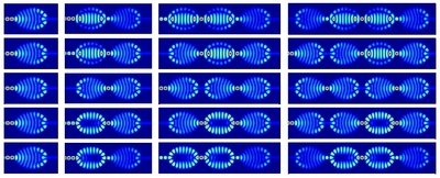
Quantum dot arrays
Assembling individual dots into coupled arrays or lattices gives rise to new features of the system's overall response, depending on the type and strength of coupling. Of particular interest are systems where the interplay between the various effects of electron transport mentioned above can be used to achieve a tunable quantum conductance, in terms of designing the size, shape and material specific features of the conducting device, as well as varying macroscopically accessible parameters such as externally applied fields, temperature, and gate voltages controlling the coupling strength between constituents.