Technology Platform CHyN Clean Room Bahrenfeld
The technology platform CHyN clean room with focus on complex nanofabrication processes is a state-of-the-art clean room facility that’s designed as a clean room ISO-Class 4 standard – an ultra-clean, particle- and dust free user lab. Equipped with cutting-edge instrumentation, it provides an ideal environment for top-level interdisciplinary research.
The lab facility is jointly operated by three organizations – Universität Hamburg (UHH), Deutsches Elektronen-Synchrotron (DESY) and Max Planck Institute for the Structure and Dynamics of Matter (MPSD). The lab is located within the Center for Hybrid Nanostructures (CHyN) Building 600 on the research campus, Science City Hamburg Bahrenfeld (SCHB).
Organization
The CHyN clean room is operated and managed by a coordinator, engineers and senior researchers from all the three organizations – UHH, DESY and MPSD – supervised by the clean room board. The board oversees the scientific directions and strategic development of the clean room.
The clean room coordinator serves as the central communication interface between users, staff, facility management, and the management board. Additionally, the coordinator oversees day-to-day operations and ensures smooth and efficient usage processes.
Available Equipment in the user lab facility
Currently, more than 20 high-precision instruments are available in the CHyN clean room facility. These can be combined into complex process chains - supported by experienced cleanroom staff - to carry out demanding research and development projects. Below is an overview of selected systems and technologies in the fields of lithography, coating, patterning, and analytical approach.
Lithographic Structuring Techniques
Electron Beam Lithography (EBL Raith Voyager)
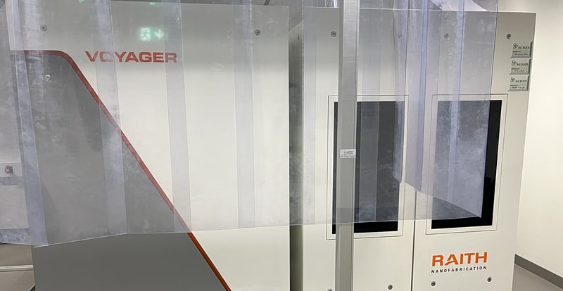
The Voyager system from Raith is a high-precision 50 kV electron beam lithography platform with a nominal accuracy of 2 nm and a minimum feature size of 6 nm (internally, we have successfully achieved 10 nm lines). It enables the exposure of substrates ranging from 5 mm to 4 inches. The Automatic Height Sensing system (update in 2024) ensures optimized focus adjustment across the entire wafer surface, minimizing focus errors and stitching artifacts.
The 2019 upgrades significantly enhance functionality: TRAXX (FBMS) enables the seamless patterning of centimeter-long paths, while PERIODIXX (MBMS) allows the fabrication of stitch-free periodic structures over large areas.
UV Lithography Mask aligner MJB4
The UV lithographic structuring is possible on the Karl Süss MJB4 mask aligner system inside the yellow room. The MJB4 is equipped with a powerful 350W high pressure mercury lamp emitting ultraviolet (UV) light in the UVA (ca. 365 nm, i-line) and UVB (ca. 313 nm, h-line) ranges. The MJB4 supports contact and proximity exposure modes. The smallest achievable feature size depends on the exposure mode: Hard contact roughly 1-micron, soft contact / proximity around 2 – 5 microns (this varies based on the gap distance). The manual mask aligner supports wafers and substrates size up to 100 mm (4”) diameter with uniformity in the illumination/ exposure over a wide range are applicable. The XYZ table allows horizontal displacement, tilting and rotation of the stage with micrometer screws. The optical alignment is handled from the top side and the vacuum is used in fixing the sample on the stage. The system is widely used for research in microfluidics, MEMS, and other microfabrication applications requiring high alignment accuracy.
Raith Picomaster: a high-resolution Laser writer
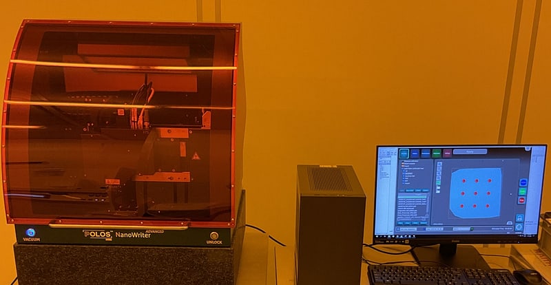
The Raith PICOMASTER comprises an advanced laser lithography system engineered for high precision, maskless lithography applications. It can accommodate a range of substrate sizes and is specifically designed for research and prototyping projects. With exceptional resolution capabilities and adjustable writing speeds, it establishes a benchmark in advanced lithography technology.
Key Technical Specification:
- Scan speed limits: maximum/ minimum scan speed of 200/20 mm/s for both directions with a movement range of 115 mm.
- Step size: minimum step size of 5 nm for the scan axis and 20 nm for the step axis respectively. The resolution can be as high as 2 nm in the ideal case.
- XY-motion limits: the substrate size can vary from 5 x 5 to 125 x 125 mm2, and it can accommodate various substrate types (sapphire, Silicon, etc.,). The exposable area is 110 x 110mm2.
Layer Deposition and Coating Method
Patterning, Implantation and Etching Techniques
List of Equipment

Photo: UHH/Akinsinde
Raith Voyager E-Beam Lithography System
Field of Application: The high-precision 50 kV electron beam lithography platform is for lithographic structuring purposes. The Voyager system has a nominal accuracy of 2 nm and a minimum feature size of 6 nm. The exposure of substrates sizes ranging from 5 mm to 4'' diameter is possible. Its recent software update automatic height sensing system allows optimized focus adjustment across the entire wafer surface, minimizing focus errors and stitching artifacts.
Location: EBL Voyager lab, CHyN Bldg. 600, RM EG. 063

Photo: UHH/Stützle
UV Lithography Mask Aligner MJB4 from Karl Süss company
Field of Application: The MJB4 model Mask aligner is typically applied as a UV lithographic structuring. With it's equipped powerful 350W high pressure mercury lamp, the emission of two characteristics ultra-violett wavelength spectrum 365 nm and 313 nm useful for micro patterning are obtainable. Contacts and proximity exposure modes are possible. The smallest achievable feature size depends on the exposure mode: Hard contact roughly 1-micron, soft contact / proximity around 2 – 5 microns. Wafers and substrates size up to 100 mm (4”) diameter with uniformity in the exposure over a wide range are applicable.
Location: CHyN Clean room, Yellow room, CHyN Bldg. 600, RM EG. 034

Photo: UHH/Stützle
Raith Picomaster: a high-resolution Maskless Laser Writing System
Field of Application: The PICOMASTER from Raith comprises an advanced laser lithography system engineered for high precision, maskless lithography applications.
Key Technical Specification:
- Scan speed limits: maximum/ minimum scan speed of 200/20 mm/s for both directions with a wide movement range of 115 mm.
- Step size: minimum step size of 5 nm for the scan axis and 20 nm for the step axis respectively. An optimal resolution as high as 2 nm is achievable.
- XY-motion limits: the substrate size can vary from 5 x 5 to 125 x 125 mm2, and various substrate types (sapphire, Silicon, etc.,). The exposable area is 110 x 110mm2.
Location: CHyN Clean room, Yellow room, CHyN Bldg. 600, RM EG. 034

Photo: UHH/Stützle
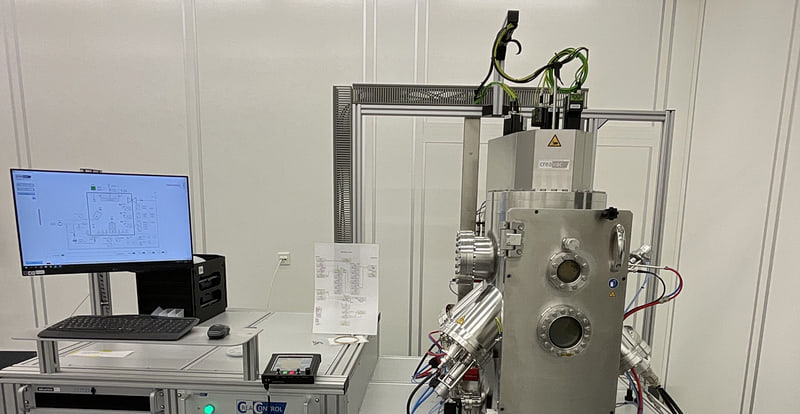
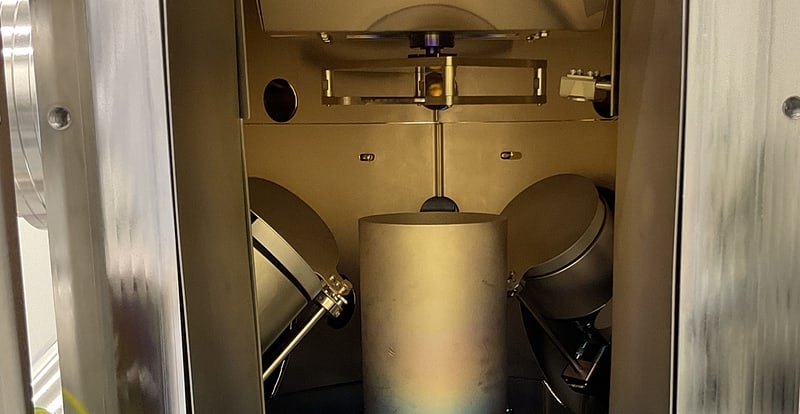
High-vacuum Coating System from Creavac: Creamet 450 E-Beam S3 Coating System
Field of Apllication: The CREAMET 450 e-beam S3 from CREAVAC is a high-vacuum coating system that operates with a multi-pocket (6 pockets) electron beam evaporator and achieves a base vacuum of < 5 X 10⁻⁷ mbar to enable high quality hin-film deposition. Substrates up to 4'' can be optimally aligned using a rotating and tilting holder, ensuring uniform coatings. Additionally, three magnetron sputter sources are available, which can operate with RF, DC, and HiPIMS technology to evaporate various materials like Au, Ti, Pt etc. Furthermore, an ion beam source allows for targeted sputtering and control of the layer morphology.
Location: CHyN Clean room, White room, CHyN Bldg. 600, RM EG. 035

Photo: UHH/Stützle
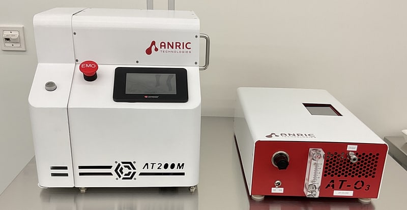
AT200M Atomic Layer Deposition (ALD) System
Field of Application: The ATM 200M is the smallest footprint ALD tool available on the market and is well-fitted for tabletop operation, and the small chamber size also ensures a high level of vacuum and small interaction volume during the deposition process. The system is equipped with one precursor and one counter-reactant, and all parts - precursor, manifold, chamber - can be heated to ensure no condensation. The deposition chamber is fitted for one 2” wafer and the deposition of thin film layers Si/SiO2, Hf/HfO2, Ti/TiO2, and Pt are possible. The typical deposition time for depositing e.g.standard recipe ca. 10nm Ti layer could last roughly 20 minutes.
Location: CHyN Clean room, White room, CHyN Bldg. 600, RM EG. 035

Photo: UHH/Stützle
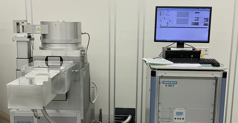
Plasma Enhanced CVD Systems SI 500D 214 from Sentech
Field of Application: The inductively coupled plasma enhanced CVD (PECVD) system SI 500D 214 from Sentech is designed for high density, low ion energy, and low-pressure plasma deposition of dielectric thin films and low-damage, very low temperature deposition of passivation layers like nitrides. The attractiveness of low etch rate, high breakdown voltage, low stress, no damage of substrate facilitates an outstanding property of the deposited layers of thin film.
The key features and benefits of the PECVD system include reproducible processes that's achievable via fully controlled via systems and process gases are NH3, SiH4 in He, CF4, O2 and Ar.
Location: CHyN Clean room, White room, CHyN Bldg. 600, RM EG. 035

Photo: UHH/Stützle
Leica EM ACE600 - TDS 02-2022 Sputter Coater
Field of Applications: The Leica ACE600 sputter coater xxxxxxxxxxxxxxxxxxxxxx
Location: CHyN Clean room, Yellow room, CHyN Bldg. 600, RM EG. 035

Photo: UHH/Stützle
DEKTAK
Field of Application: XXXXXXXXXX.
Location: CHyN Clean room, Yellow room, CHyN Bldg. 600, RM EG. 034

Photo: UHH/Stützle
Ellipsometer
Field of Applications: The Leica ACE600 sputter coater xxxxxxxxxxxxxxxxxxxxxx
Location: CHyN Clean room, Yellow room, CHyN Bldg. 600, RM EG. 035

Photo: UHH/Stützle
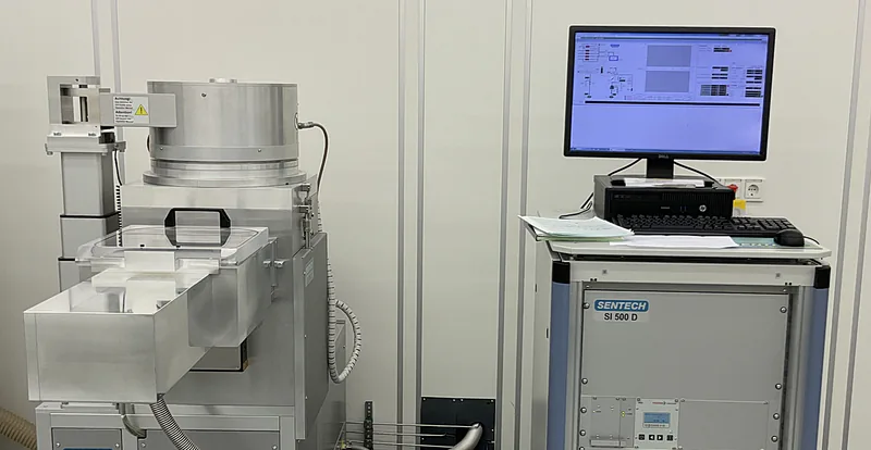
Reactive Ion Etcher SI 500 215
Field of Applications: The SI 500 ICP-RIE from the company Sentech is a high-end plasma etch system that uses an inductively coupled plasma source with low ion energy for low-damage dry etch and nano structuring of different substrates mostly wafers, sapphire and glass. The system has its unique feature in processes reproducibility achievable through the integrated full controlled vacuum system, different levels of automation ranging from load-lock loading to the process chamber. The following standard reactive process gases SF6, CHF3, C4F8, O2 and Ar are utilized for the dry etching process.
Location: CHyN Clean room, Yellow room, CHyN Bldg. 600, RM EG. 035

Photo: UHH/Akinsinde
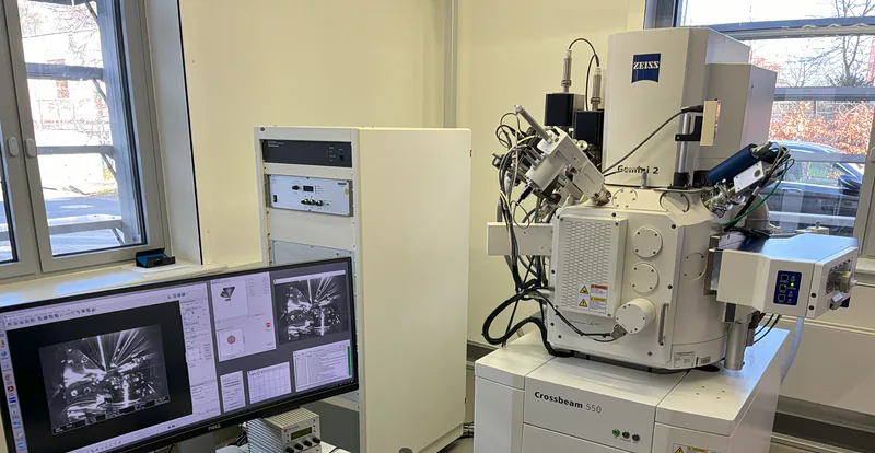
FIB-SEM - ZEISS Crossbeam 550 coupled FIB
Field of Application: The FIB-SEM (ZEISS Crossbeam 550, is used in investigating the structure and morphology - high-resolution imaging with resolution below 10 nm of all kinds of conductive and non-conductive materials is possible - of different specimens by scanning electron microscopy (SEM) in combination with optional focused ion beam (FIB) milling for patterning purpose. Also, elemental analysis of the specimen material can be conducted by energy-dispersive X-ray spectroscopy (EDS). The sample analysis enhanced by EDS to study the elemental composition and purity of thin films, micro- and -nanostructures.
Location: SEM-FIB lab, CHyN Bldg. 600, RM EG. 060
List of Equipment
Photo: UHH/Akinsinde
Raith Voyager Elektronenstrahl Lithografie
Anwendungsbereiche: Die Elektronenstrahllithografie mit dem Raith Voyager-System ermöglicht durch ihre hohe Präzision die Herstellung feinster Strukturen bis in den Nanometerbereich. Mit einer Spannung von 50 kV, einer nominellen Genauigkeit von 2 nm und einer realisierbaren Strukturbreite bis hinunter zu 10 nm eignet sich dieses System ideal für komplexe Lithografiemuster. Dank automatisierter Höhensensorik und Funktionen wie TRAXX und PERIODIXX lassen sich strukturierte Pfade und periodische Muster über große Flächen stitch-frei realisieren.
Standort: EBL Voyager Labor, CHyN Geb. 600, RM EG. 063, SCHB
Photo: UHH/Stützle
UV Lithografie Mask Aligner MJB4
Anwendungsbereiche: Im Bereich der UV-Lithografie kommt der Mask Aligner Karl Süss MJB4 zum Einsatz. Dieses System eignet sich besonders für mikrofluidische Anwendungen, MEMS und weitere mikrostrukturierte Designs. Mit Belichtungsmodi wie Kontakt und Proximity lassen sich Strukturen ab etwa 1 µm realisieren, wobei eine hochpräzise Ausrichtung durch einen XYZ-Tisch gewährleistet ist.
Standort: CHyN Reinraum, Gelblichtraum, CHyN Geb. 600, RM EG. 034,SCHB
Photo: UHH/Stützle
Raith Picomaster: Hochauflösender Maskenloser Laserschreiber
Anwendungsbereiche: Der Raith PICOMASTER ist leistungsfähiger maskenloser Laserwriter für die hochpräzise Belichtung verschiedenster Substrattypen. Mit einer Schreibauflösung von bis zu 2 nm auf versdchiedene Substraten wie SiO2 Wafer, Glas usw. und einer flexiblen Substratgröße bis 125 mm² bietet er herausragende Möglichkeiten für Forschung und Prototyping.
Standort: CHyN Reinraum, Gelblichtraum, CHyN Geb. 600, RM EG. 034, SCHB
Photo: UHH/Stützle
DEKTAK
Field of Application: XXXXXXXXXX.
Location: CHyN Clean room, Yellow room, CHyN Bldg. 600, RM EG. 034
Photo: UHH/Stützle
Hochvakuum Beschichtungsanlage: Creamet 450 Elektronenstrahl S3 Beschichtungssystem
Anwendungsbereiche: Für hochpräzise Beschichtungsprozesse steht die CREAMET 450 E-Strahl S3 von CREAVAC zur Verfügung. Dieses Hochvakuum-System ermöglicht sowohl die Elektronenstrahlverdampfung als auch das Sputtern verschiedenster Materialien – unterstützt durch moderne Technologien wie RF-, DC- und HiPIMS-Verfahren. Die integrierte Ionenstrahlquelle erlaubt eine gezielte Beeinflussung der Schichtmorphologie, während die intelligente CREACONTROL-Steuerung eine stabile, reproduzierbare Prozessführung sicherstellt.
Standort: CHyN Reinraum, weiße Raum, CHyN Geb. 600, RM EG. 035,SCHB
Photo: UHH/Stützle
AT200M Atomen Lagenabcheidung (ALD) System
Anwendungsbereiche: ein kompaktes ALD-Gerät (Atomlagenabscheidung), das für die hochpräzise Abscheidung ultradünner Schichten auf 2-Zoll-Wafern konzipiert ist. Mit beheizbaren Komponenten und einer Auswahl an bis zu drei Präkursoren (z. B. Pt, Ti, Hf, Si) sowie Reaktionsmitteln wie H₂O, O₂ und O₃ eignet sich das System für die Herstellung funktionaler Schichten wie Al₂O₃, TiO₂ oder SiO₂ mit höchster Homogenität.
Standort: CHyN Reinraum, weiße Raum, CHyN Geb. 600, RM EG. 035, SCHB
Photo: UHH/Stützle
Induzierte Plasma CVD Systeme SI 500D 214
Anwendunsgereiche: Für die Abscheidung von Passivierungsschichten kommt das PECVD-System SI 500D 214 von Sentech zum Einsatz. Die plasmaunterstützte chemische Gasphasenabscheidung erlaubt die Herstellung dichter, spannungsarmer dielektrischer dünnen Schichten bei niedrigen Temperaturen.
Standort: CHyN Clean room, White room, CHyN Geb. 600, RM EG. 035,SCHB
Photo: UHH/Stützle
Leica EM ACE600 - TDS 02-2022 Sputter Coater
Field of Applications: The Leica ACE600 sputter coater xxxxxxxxxxxxxxxxxxxxxx
Location: CHyN Clean room, Yellow room, CHyN Bldg. 600, RM EG. 035
Photo: UHH/Stützle
Ellipsometer
Field of Applications: The Leica ACE600 sputter coater xxxxxxxxxxxxxxxxxxxxxx
Location: CHyN Clean room, Yellow room, CHyN Bldg. 600, RM EG. 035
Photo: UHH/Stützle
Reaktive Ionen Ätzen SI 500 215
Anwendungsbereiche: Für das reaktive Ionentiefätzen (RIE) kommt das SI 500 ICP-RIE-System von Sentech zum Einsatz. Mit seiner induktiv gekoppelten Plasmaquelle, der Planar Triple Spiral Antenna (PTSA), erzeugt es ein homogenes Plasma mit hoher Ionendichte bei niedriger Energie – ideal für schonendes, präzises Strukturieren. Die temperaturgeregelte Substratelektrode sowie das automatisierte Vakuum- und Gassystem ermöglichen reproduzierbare Prozesse bei höchster Kontrolle.
Standort: CHyN Reinraum, Gelblichtraum, CHyN Geb. 600, RM EG. 035,SCHB
Photo: UHH/Akinsinde
FIB-SEM - ZEISS Crossbeam 550 gekoppelte Fokussierte Ionenstrahl (FIB)
Anwendungsbereiche: Zur hochauflösenden Strukturierung und Analyse steht das ZEISS Crossbeam 550 zur Verfügung – ein kombiniertes FIB-SEM-System (Focussed Ion Beam / Scanning Electron Microscope). Dieses Instrument ermöglicht neben der Bildgebung im Sub-10-nm-Bereich auch gezielte Materialabtragungen und Querschnittanalysen mithilfe eines Gallium-Ionenstrahls. Ergänzt wird das System durch ein EDS-Modul zur Elementanalyse. Es eignet sich besonders zur Untersuchung mikro- und nanostrukturierter Proben sowie zur Charakterisierung funktionaler Dünnschichten und komplexer Zell-Nanostruktur-Interaktionen
Standort: FIB Labor, CHyN Geb. 600, RM EG. 060, SCHB